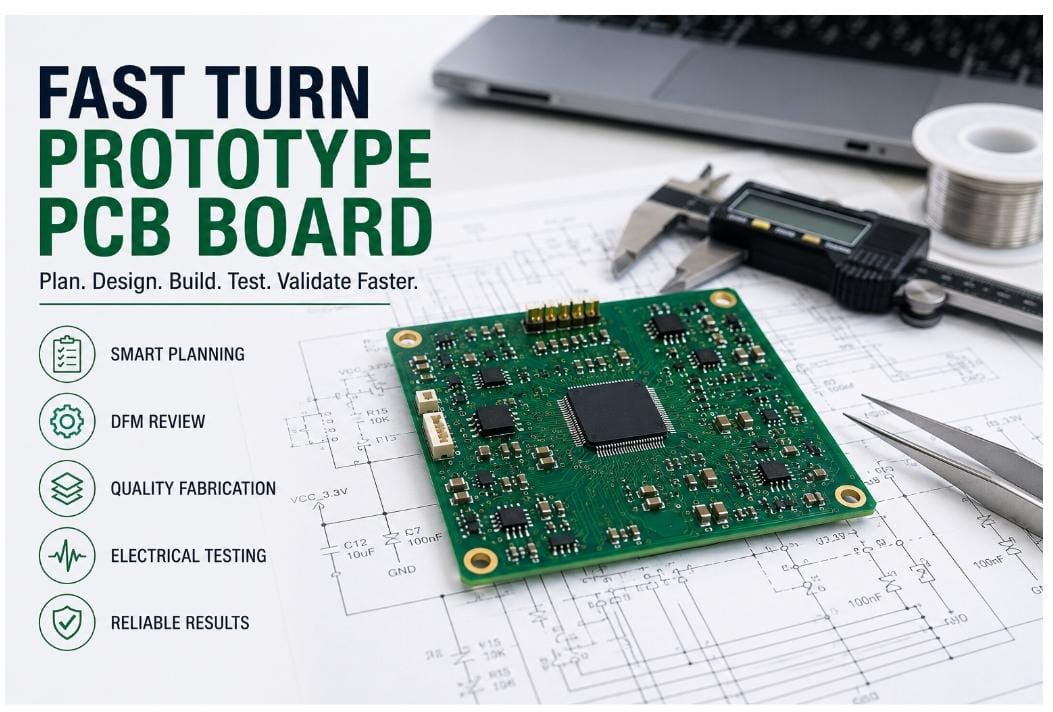
Bringing a new electronic product from concept to production requires careful validation at every stage of development. Before investing in large production volumes, engineering teams use prototype PCBs to verify circuit functionality, evaluate mechanical fit, confirm manufacturability, and identify potential design improvements. A well planned prototype phase helps reduce technical risks while shortening the overall product development cycle.
Submitting a fast turn prototype PCB board for fabrication involves much more than exporting Gerber files. Engineers should prepare complete manufacturing documentation, review Design for Manufacturability (DFM), verify stackup requirements, select appropriate materials, and define testing procedures before releasing a design for fabrication. Investing time in these activities early often reduces redesign cycles and improves prototype quality.
This guide outlines practical engineering practices that help development teams prepare PCB prototypes efficiently while supporting a smoother transition into production.
Establish Clear Prototype Objectives
Every prototype should have clearly defined engineering goals before fabrication begins.
Rather than treating the prototype as a simple proof of concept, engineering teams should identify exactly what the board is intended to validate.
Common objectives include:
- Electrical functionality
- Signal integrity
- Thermal performance
- Mechanical enclosure fit
- Firmware validation
- Assembly evaluation
- Production readiness
Clearly documented objectives help determine the appropriate manufacturing processes, materials, inspection methods, and testing requirements.
A prototype designed for electrical validation may not require the same manufacturing specifications as one intended for environmental testing or customer demonstrations.
Prepare Complete Manufacturing Documentation
Manufacturing delays frequently occur because engineering documentation is incomplete rather than because of fabrication capacity.
A comprehensive documentation package normally includes:
- Gerber or ODB++ files
- NC drill files
- Fabrication drawings
- PCB stackup documentation
- Bill of Materials (for assembled prototypes)
- Pick and place files
- Assembly drawings
- Special fabrication notes
Providing accurate documentation allows manufacturers to review the project efficiently while reducing clarification requests during production.
Documentation should always be reviewed internally before release to ensure consistency across all files.
Complete a Design for Manufacturability Review
Design for Manufacturability helps identify design features that may complicate fabrication or assembly.
A thorough DFM review typically evaluates:
- Minimum trace width and spacing
- Annular ring dimensions
- Drill sizes
- Copper clearances
- Solder mask openings
- Component spacing
- Panel utilisation
- Fabrication tolerances
Addressing these issues before fabrication generally improves manufacturing yield while reducing engineering revisions.
Early collaboration with the manufacturer also provides valuable feedback that can simplify production without affecting electrical performance.
Review the PCB Stackup
The PCB stackup directly influences electrical characteristics, board thickness, impedance control, and manufacturing complexity.
Changing the stackup after routing often results in unnecessary redesign work.
Before prototype release
Select Materials That Match Prototype Requirements
Material selection affects much more than lead time. The laminate, copper weight, surface finish, and dielectric properties all influence electrical performance, thermal behaviour, and long term reliability.
When planning a prototype, engineers should evaluate:
- Base laminate type
- Copper thickness
- Surface finish
- Overall board thickness
- Dielectric material
- Thermal requirements
- Controlled impedance requirements
Whenever specialised materials are required, confirming availability before releasing the design helps prevent unexpected manufacturing delays.
Material selection should balance electrical performance with manufacturing practicality, especially when the prototype is expected to transition into volume production.
Define Testing Requirements Before Fabrication
Testing should be planned during the design stage rather than after the prototype has been manufactured.
Early planning allows manufacturers to prepare the appropriate inspection and testing processes throughout fabrication.
Common prototype testing methods include:
- Electrical continuity testing
- Flying probe testing
- Functional testing
- Open and short circuit verification
- Controlled impedance verification
- In circuit testing where applicable
Clearly documenting testing expectations helps ensure the finished prototype supports the intended engineering validation activities.
Inspection and Quality Verification
Comprehensive inspection helps verify that the manufactured PCB matches the released engineering documentation before assembly begins.
Rather than relying only on a final inspection, manufacturers typically perform quality checks throughout the fabrication process.
Common inspection procedures include:
- Automated Optical Inspection (AOI)
- Electrical testing
- Hole size verification
- Copper feature inspection
- Solder mask inspection
- Surface finish verification
- Dimensional measurement
For multilayer boards, cross section analysis may also be used to verify copper plating quality, layer registration, and dielectric thickness.
A structured inspection process provides engineering teams with greater confidence when evaluating prototype performance.
Maintain Effective Revision Control
Prototype development often involves several engineering revisions before production begins.
Without proper revision management, outdated manufacturing files can accidentally be released, leading to unnecessary delays and additional fabrication costs.
Good revision control includes:
- Unique revision identifiers
- Controlled engineering documentation
- Updated fabrication drawings
- Revision history records
- Approved Bills of Materials
- Archived manufacturing packages
Maintaining accurate revision records improves communication between engineering, procurement, assembly, and manufacturing teams.
Common Prototype Planning Mistakes
Many prototype issues originate during project planning rather than during fabrication.
Some of the most common mistakes include:
- Releasing incomplete manufacturing files
- Skipping Design for Manufacturability review
- Modifying the PCB stackup after routing
- Selecting unavailable materials
- Defining testing requirements too late
- Poor revision management
- Missing fabrication notes
- Incomplete engineering documentation
Avoiding these problems early helps reduce prototype iterations while improving manufacturing efficiency.
Prototype Readiness Checklist
Before submitting a prototype PCB for fabrication, engineering teams should verify that all critical planning activities have been completed.
| Planning Area | Verification |
| Prototype objectives | Clearly documented |
| Manufacturing documentation | Complete and reviewed |
| DFM review | Completed |
| Material selection | Confirmed |
| PCB stackup | Finalised before routing |
| Testing requirements | Defined |
| Inspection plan | Established |
| Revision control | Updated |
| Manufacturing notes | Included |
Using a structured checklist reduces the likelihood of delays while improving communication between engineering and manufacturing teams.
Final Thoughts
A successful PCB prototype is the result of careful engineering preparation rather than rapid fabrication alone. Complete manufacturing documentation, thorough Design for Manufacturability reviews, appropriate material selection, stackup planning, inspection procedures, testing strategies, and effective revision control all contribute to higher quality prototypes and a smoother development process.
Treating the prototype as an important engineering milestone rather than simply an early production sample allows teams to identify potential manufacturing challenges before committing to larger production volumes. This structured approach reduces redesign cycles, improves collaboration between design and manufacturing teams, and supports a more efficient transition into production.
For organisations developing new electronic products, Fast Turn PCB provides prototype PCB manufacturing supported by engineering review, quality inspection, and production planning. Manufacturing capabilities, material availability, achievable lead times, and testing processes should always be confirmed after reviewing the specific design requirements and project objectives.
By following established engineering practices throughout the prototype phase, development teams can improve product quality, minimise project risks, and move confidently from design validation to successful production.