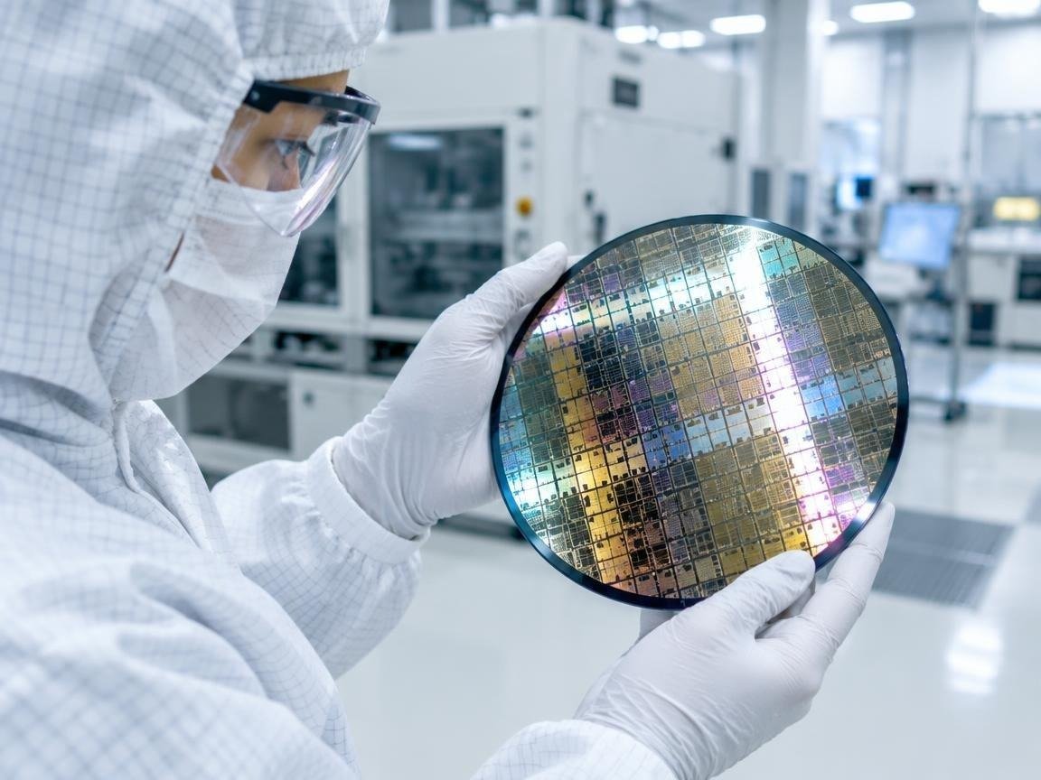
The Critical Role of Photomasks and Reticles in Advanced Lithography
In the complex world of semiconductor manufacturing, precision is paramount. A single microscopic flaw can lead to massive production losses. This impacts the global technology supply chain.
At the heart of this intricate process are reticles, also known as photomasks. These are not just pieces of glass. They are the master blueprints that define every circuit pattern on a microchip.
These critical components are incredibly valuable and sensitive. They demand extreme protection from defects, contamination, and handling damage. Safeguarding these high-value assets is crucial for maintaining wafer yield and ensuring reliable chip production.
In this guide, we will explore the vital role of reticles in photolithography. We will delve into how these essential tools are protected throughout their lifecycle. This includes the advanced engineering of specialized reticle carriers—components so critical that dedicated reticle carriers manufacturers focus solely on their design and production. We will also cover stringent contamination control methods and rigorous quality inspection processes. Understanding these elements is key to protecting the integrity of our semiconductor manufacturing.
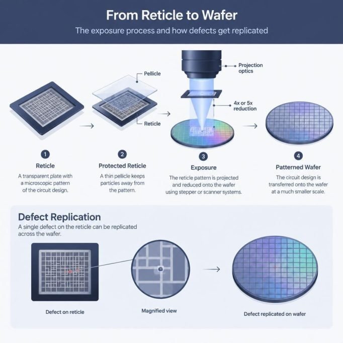
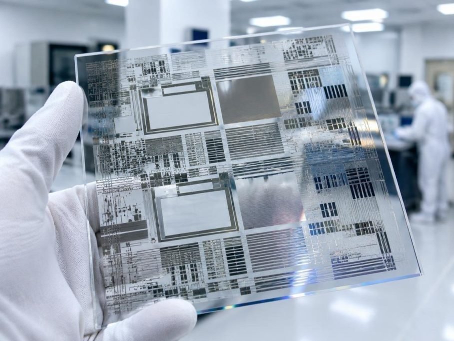
At its core, a reticle (or photomask) is a transparent plate, typically made of high-purity fused silica, with a microscopic pattern of the integrated circuit design etched onto a thin layer of opaque material, usually chromium. This pattern serves as the master template for transferring circuit designs onto silicon wafers during the photolithography process. In modern stepper or scanner systems, the reticle’s pattern is projected and reduced by a specific ratio (commonly 4x or 5x) onto the wafer, allowing for the creation of incredibly fine features.
To protect this delicate pattern from airborne particles and other contaminants, a thin, transparent membrane called a pellicle is stretched over the reticle’s patterned surface. This pellicle creates a standoff distance, ensuring that any particles settling on its surface are out of the optical system’s focal plane, thus preventing them from being printed onto the wafer. The precision required for these components is immense; even a nanometer-scale defect can have catastrophic consequences for chip functionality.
The relationship between a reticle’s features and the final features on the wafer is not always linear, especially at advanced technology nodes. This non-linearity is often quantified by the Mask Error Enhancement Factor (MEEF), which describes how a small variation on the reticle can be magnified on the wafer. Understanding and managing MEEF dynamics is crucial for achieving tight Critical Dimension (CD) control.
Optical vs. EUV Reticle Fundamentals
The evolution of lithography has led to significant changes in reticle technology. Traditional deep ultraviolet (DUV) lithography, utilizing wavelengths like 193nm (including immersion lithography), relies on transmission reticles. These reticles are designed to allow light to pass through the clear areas of the fused silica substrate, with the chromium pattern absorbing the light in the opaque regions.
However, with the advent of Extreme Ultraviolet (EUV) lithography for sub-10nm nodes, the fundamental nature of reticles transformed. EUV light, with its 13.5nm wavelength, is absorbed by almost all materials, including fused silica. Therefore, EUV lithography employs reflective reticles. These specialized masks are built upon a low-thermal-expansion substrate, coated with a multilayer stack of molybdenum and silicon (Mo/Si). This multilayer acts as a Bragg reflector, designed to reflect the 13.5nm EUV light where the pattern is clear, while an absorber layer (e.g., tantalum nitride) defines the opaque regions. The shift to reflective optics introduces unique challenges in design, manufacturing, and inspection.
Here’s a comparison of these two critical reticle types:
Feature Optical DUV Reticles (e.g., 193nm) EUV Reflective Masks (13.5nm) Light Interaction Transmission Reflection Substrate Material Fused Silica Low Thermal Expansion Material (LTEM) Pattern Layer Chromium (Cr) Mo/Si Multilayer (Reflector) + Absorber (e.g., TaN) Pellicle Transmissive (organic film) Currently under development (must be EUV transparent) Defect Sensitivity Surface particles, pattern defects Surface particles, pattern defects, subsurface defects, phase defects Inspection DUV light, e-beam Actinic EUV, e-beam Defect Propagation and Wafer Yield Risk
The extreme precision of semiconductor manufacturing means that even the smallest defect on a reticle can have disproportionately large consequences. A single microscopic particle, a tiny scratch, or an unintended pattern deviation on the reticle will be replicated across every single die exposed on the wafer. These are known as repeater defects.
Consider a scenario where a reticle is used to expose thousands of wafers, each containing hundreds of individual chips. A defect that might be barely visible to the naked eye on the reticle could lead to millions of defective chips over the reticle’s lifetime, resulting in massive die scrap and significant economic losses. The impact is further exacerbated by the Mask Error Enhancement Factor (MEEF), where a small reticle CD error can lead to a much larger CD error on the wafer, pushing the device out of specification.
Maintaining tight control over Critical Dimension (CD) variation on the reticle is paramount. Any deviation can shrink the usable process window—the range of lithography parameters (like focus and exposure) within which acceptable patterns can be printed. When reticle defects or CD errors consume too much of this window, the process becomes unstable, leading to reduced yield and increased manufacturing costs. Preventing these defects from ever reaching the wafer is a continuous, multi-faceted challenge.
Engineering Standards for Semiconductor Reticle Carriers
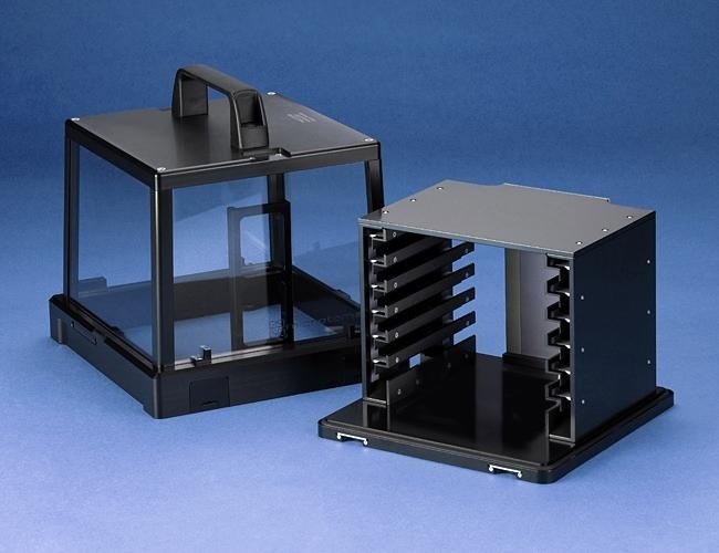
Given the immense value and sensitivity of reticles, their physical protection during transport, storage, and loading into lithography tools is non-negotiable. This is where specialized reticle carriers come into play. These carriers are not merely boxes; they are precision-engineered enclosures designed to meet stringent industry specifications, primarily defined by SEMI standards.
These standards dictate everything from mechanical interfaces to material properties, ensuring compatibility across different equipment manufacturers and safeguarding the reticle from its environment. A key requirement is maintaining an ultra-clean internal environment, often equivalent to a Class 1 cleanroom or better, to prevent particle contamination. Carriers must also be compatible with SMIF (Standard Mechanical Interface) systems, allowing for automated, hands-free transfer of reticles between storage systems and lithography tools without exposing them to the ambient fab environment. This particle isolation is critical for preventing defects.
Materials and ESD Protection in Semiconductor Reticle Carriers
The selection of materials for reticle carriers is a meticulous process, balancing durability, cleanliness, and protective properties. Common materials include high-performance polymers like PEEK (Polyetheretherketone) and carbon-filled composites. These materials are chosen not only for their mechanical strength and low outgassing characteristics but also for their ability to provide ESD (Electrostatic Discharge) protection. Static electricity can attract particles to the reticle surface or, in severe cases, damage sensitive components. Carriers are engineered to prevent static buildup, often achieving rapid static decay times and maintaining a specific surface resistivity to safely dissipate charges.
The design often incorporates concepts like a Faraday cage, where conductive materials form an enclosure to shield the reticle from external electromagnetic fields. Furthermore, carriers may include features for UV attenuation to protect certain reticle types or pellicles from light exposure during storage. Strict controls are also in place to prevent outgassing, where volatile organic compounds (VOCs) from carrier materials could condense on the reticle surface and cause chemical contamination.
Dual-Pod Architecture for EUV Reticle Transport
EUV reticles present an even greater challenge for protection due to their reflective nature and extreme sensitivity to contamination, particularly hydrocarbons, which can polymerize under EUV light. To address this, a specialized dual-pod architecture has become standard for EUV reticle transport and storage.
This system consists of two main components: an inner pod and an outer pod shell. The inner pod, often constructed from a high-purity metal enclosure, directly houses the EUV reticle. This metal pod is designed to be hermetically sealed and is typically kept under vacuum purging or an inert gas environment to prevent any particulate or molecular contamination. The inner pod is only opened within the highly controlled environment of the EUV lithography tool.
The outer pod, usually made of polymer, provides mechanical protection and an interface for robotic handling in the fab. It encapsulates the inner pod, protecting it from the ambient cleanroom environment. Critical design considerations for these dual-pods include managing pressure differential during vacuum cycles and ensuring optimal slit seal conductance for efficient purging and minimal particle ingress. This elaborate system ensures the ultra-clean environment necessary for EUV reticles from the mask shop to the lithography scanner.
Contamination Control, Purge Systems, and Fab Automation
Beyond the carriers themselves, a comprehensive ecosystem of contamination control and automation exists within the semiconductor fab to protect reticles. This includes sophisticated storage solutions, environmental controls, and integrated tracking systems.
Automated reticle stockers are robotic libraries designed to store hundreds or thousands of reticles in a controlled, clean environment. These stockers minimize human interaction, a major source of contamination, and provide rapid access to reticles as needed. Integration with the fab’s MES (Manufacturing Execution System) allows for real-time tracking of each reticle’s location, usage history, and inspection status.
Within these stockers and during transport, various purge systems are employed. XCDA (Extra Clean Dry Air) or high-purity nitrogen purge are commonly used to continuously flush the reticle environment, actively removing airborne particles and molecular contaminants. Advanced particle filtration systems ensure that the incoming purge gases are ultra-clean, preventing any new contaminants from being introduced. These measures are crucial in combating chemical outgassing from fab materials and equipment, which can deposit residue on reticle surfaces.
Automated Handling and Semiconductor Reticle Carriers
The journey of a reticle through a modern semiconductor fab is largely automated. Robotic systems, equipped with delicate robotic end-effectors, precisely handle reticle carriers and load them into lithography tools or inspection equipment. These systems are engineered with vibration dampening mechanisms to prevent any mechanical shock or movement that could dislodge particles or damage the reticle.
The contact force of robotic grippers is carefully calibrated to ensure secure handling without over-stressing the carrier or its contents. Each reticle carrier is equipped with unique identifiers, such as barcode serialization, allowing the MES to track its exact location and history. Many carriers also feature info pads—configurable plugs or electronic tags that communicate critical information (e.g., reticle ID, pellicle status) to the processing tool, enabling automated verification and preventing mix-ups. In some cases, these info pads can even trigger a tool lockout if a reticle is not approved for a particular process step, adding another layer of error prevention.
Purging Protocols and Moisture Mitigation
Maintaining an optimal micro-environment around the reticle is a continuous battle against ambient conditions. Purging protocols are meticulously designed to control relative humidity and mitigate the impact of airborne molecular contamination (AMC). High humidity can lead to water adsorption on surfaces, which can then react with other contaminants to form damaging residues, such as sulfate crystal growth on the reticle or pellicle.
To combat this, carriers and storage systems are equipped with breather filters that allow for pressure equalization while filtering out particles. For more sensitive processes, vacuum load-locks are used to transition reticles between atmospheric pressure and vacuum environments without introducing contaminants. The use of ultra-dry purge gases like nitrogen helps to actively remove moisture.
Here are some key environmental purge controls:
- Continuous Inert Gas Purge: Flowing dry nitrogen or XCDA through reticle carriers and storage cabinets.
- Molecular Filtration: Utilizing chemical filters to remove AMCs (e.g., acids, bases, organic compounds).
- Pressure Control: Maintaining a slight positive pressure within carriers to prevent inward leakage of contaminated air.
- Vacuum Sealing: For EUV reticles, inner pods are often sealed under vacuum or inert gas to eliminate contamination.
- Temperature and Humidity Control: Strict environmental control within stockers and lithography areas.
Reticle Quality Inspection and Lifecycle Management
The integrity of a reticle is not a one-time check; it’s a continuous process throughout its operational lifecycle. From its initial manufacturing to its eventual retirement, a reticle undergoes rigorous inspection routines and requalification cycles. Upon delivery from the mask shop, a new reticle is thoroughly inspected for defects and pattern accuracy. As it accumulates usage cycles in the lithography tool, periodic requalification cycles are performed to detect any new defects, contamination, or pattern degradation.
Modern fabs leverage advanced technologies like AI defect detection to analyze inspection images, identifying subtle flaws that human inspectors might miss and reducing the time required for review. Two primary methods for pattern verification are employed: die-to-database inspection compares the reticle pattern to the original design data, ensuring fidelity, while die-to-die metrology compares repeating patterns on the reticle itself, effectively finding random defects. This continuous vigilance ensures that only defect-free reticles are used in production.
Metrology and Defect Inspection Workflows
The tools and workflows for reticle inspection are highly specialized and continuously evolving to keep pace with shrinking feature sizes. For optical reticles, advanced DUV inspection systems and e-beam inspection are standard. E-beam inspection offers superior resolution, capable of detecting sub-nanometer defects that are critical for advanced nodes.
For EUV reticles, the challenge is even greater. Actinic EUV inspection uses the same 13.5nm wavelength light as the lithography tool to detect defects that are only visible under EUV illumination, such as phase defects within the multilayer stack. Additionally, CD-SEM (Critical Dimension Scanning Electron Microscope) tools are used for precise measurement of pattern dimensions on the reticle. A significant focus in these workflows is on false positive reduction—minimizing the number of benign features or noise signals incorrectly flagged as defects, which can consume valuable engineering time. The ultimate goal is accurate pattern verification that directly correlates to wafer yield.
Pod Cleaning and Maintenance Protocols
The cleanliness of the reticle carrier directly impacts the cleanliness of the reticle itself. Therefore, strict pod cleaning and maintenance protocols are essential. Carriers are regularly cleaned using specialized processes, often involving a DI (deionized) water rinse followed by non-contact drying methods (e.g., nitrogen blow-off) to prevent water spots or particle deposition.
Critical components, such as door seals and breather filters, have defined replacement schedules, with door seal replacement typically occurring every 12 months or after a certain number of cycles to maintain sealing integrity. Fabs implement robust consumable tracking systems to manage these replacements. Establishing a particulate baseline for clean carriers and monitoring it regularly ensures that the carriers themselves are not a source of contamination. This proactive maintenance prevents the carriers from becoming a vector for cross-contamination, safeguarding the pristine condition of the reticles they protect.
Frequently Asked Questions About Reticle Protection
What is the primary purpose of a semiconductor reticle carrier?
A semiconductor reticle carrier primarily serves to protect the reticle from its environment. This includes particle isolation to prevent contamination, ESD suppression to dissipate static charges, physical shock damping to protect against mechanical damage, and providing a clean, sealed environment for cleanroom transport and storage.
How do EUV reticle pods differ from standard optical photomask pods?
EUV reticle pods are significantly more complex. They typically feature a dual-pod system with an inner metal enclosure that directly houses the EUV reticle. This inner pod is designed for vacuum compatibility and is often purged with inert gas, ensuring an ultra-clean environment. They also incorporate mechanisms for precise pressure equalization during vacuum cycling, which is not required for standard optical pods.
Why is reticle carrier maintenance essential for fab yield?
Reticle carrier maintenance is crucial for fab yield because poorly maintained carriers can become a source of contamination. Degrading seals or dirty internal surfaces can lead to cross-contamination, resulting in repeater defects on wafers. Regular maintenance, including cleaning and component replacement, ensures seal integrity and proper outgassing control, directly preventing yield loss from reticle-borne defects.
Conclusion
The reticle, or photomask, stands as an indispensable artifact in the intricate dance of semiconductor manufacturing. It is far more than a mere stencil; it is the genesis of every microchip, demanding unparalleled levels of protection and precision. As we push the boundaries of lithography into sub-wavelength and EUV regimes, the challenges of safeguarding these critical components only intensify.
The synergy of advanced materials in reticle carriers, sophisticated automation, and stringent contamination control systems forms a robust defense against the myriad threats to reticle integrity. From the dual-pod architecture for EUV to AI-enhanced inspection and meticulous maintenance protocols, every element plays a vital role in protecting these high-value assets. This integrated approach not only acts as a yield safeguard but also enables the continuous advancement of the lithography roadmap, ensuring the longevity and reliability of semiconductor manufacturing for years to come.